FUTURE OF NANOELECTRONICS

INTRODUCTION TO NANOELECTRONICS

Electronics has been a foremost driver of the scientific and technological progress that has made a major contribution to social and economic growth worldwide since the middle of the 20th century. Some of the notable recent success stories — mobiles, telephones, digital media, computing, and networking (especially the Internet), safer and more efficient vehicles with less-polluting engines, and medical systems — illustrate the crucial innovative role that microelectronics has played. And the innovation of technology from micro- to nanoelectronics can only increase this key position.
WHAT IS NANO-ELECTRONICS?
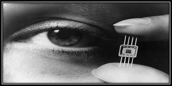
Nanoelectronics can be defined as electronics on the deep submicron level that is with circuit dimensions of less than 0.1 micron. The term covers both the manufacturing of even smaller and hence higher performance of existing semiconductor devices and advances in molecular electronics that involve exploiting of single atoms or molecules. For more than fifty years, miniaturization of transistors, which are the building blocks of all electronic chips, has been driving the semiconductor industry.

The following trend of miniaturization and doubling of the transistor density in a chip every two years and is popularly known as Moore’s law. In general, reducing transistor sizes facilitates realizing electronic products with a higher speed and lower power consumption at a lower cost.
Moreover, we have now entered a new era of computing, the applications such as artificial intelligence, autonomous systems, big data, Internet of Things, 5G, etc. have taken the centre stage of computing. These applications consume and generate a tremendous amount of data and demand unprecedented high computational power. It is now evident that the state-of-the-art transistors, even when scaled down to very small dimensions, cannot fulfil the requirements of the new era computing. The demand for energy-efficient computation from the newer applications has made the research on nano-electronic devices necessary.
MOORE’S LAW -
Moore’s law is the observation that the number of transistors in a dense integrated circuit (IC) doubles about every two years. Moore’s law is an observation and projection of a historical trend. Rather than a law of physics, it is an empirical relationship linked to gains from experience in production.

TUNNEL TRANSITOR -
Among the exploratory devices, tunnel transistors operate on the principle of quantum tunnelling, a phenomenon in which an electron can cross a barrier even though it has energy less than the barrier. The tunnelling phenomenon is like throwing a ball against a hard wall and the ball reaching the other side of the wall without any apparent sign of a hole in the wall. Such a phenomenon seems weird from our daily experience, but in the realms of electrons, tunnelling phenomenon does occur.
In tunnel transistors, by providing a high barrier, the leaky electrons are stopped. By exploiting the tunnelling phenomenon, a tunnel transistor switches-on even when a very small voltage is applied. Consequently, tunnel transistors can be ten times more energy-efficient than the state-of-the-art transistors and are dubbed as “green transistors”. However, due to high obstruction to current conduction, tunnel transistors exhibit low speed.
MOLECULAR TRANSISTOR -
Molecular transistor consists of a single molecule for current conduction and represents the ultimate limit of miniaturization. Though, currently, the performance of a molecular transistor is inferior to the state-of-the-art transistor, with more research molecular transistors can be quite interesting. Moreover, researchers are trying to exploit another property of an electron known as “spin”. Traditionally, transistors utilize the “charge” of an electron for information processing. However, the spin of an electron can also be manipulated in a transistor and be utilized for information processing.
WHAT IS CMOS?
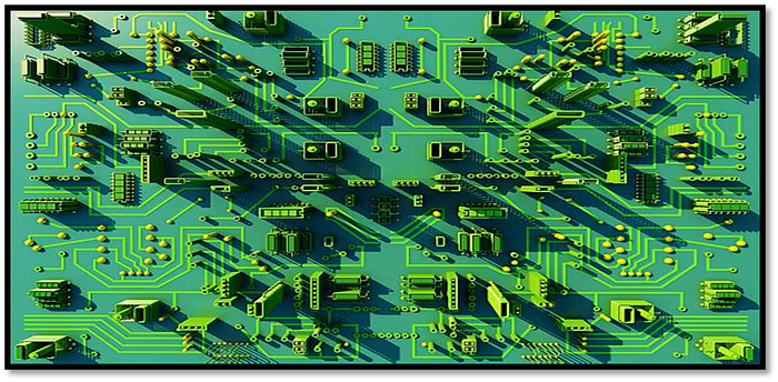
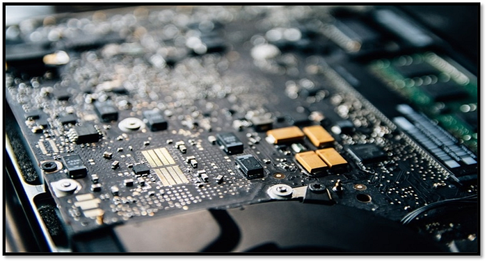
Complementary metal oxide semiconductor (CMOS)technology dominates manufacture of integrated circuits today. Its energy efficiency makes it possible to integrate many more CMOS gates on a chip than those made with alternative technologies, so offering much higher functionality. As a result, CMOS is currently the mainstream technology for microprocessors, memory, and logic circuits. While the size of the electronic elements in integrated circuits is shrinking and complexity is strongly increasing to combine more functions on a single chip. These include operation with ultra-high clock speeds, ultra-low electric power consumption and functioning in very harsh environments. This leads to diversification of the standard (CMOS) technology into sub-families.
One strong industry requirement is that the production processes be compatible with silicon wafer technologies to allow a smooth transfer in manufacturing. Alternatives or complements to CMOS, such as spin electronics, molecular electronics, and quantum computing, also exist and are in the early stages of research and development. They are promising directions to find new device concepts.
APPLICATIONS
1. Nano-scale medical diagnostics and treatment
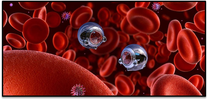
Nanoelectronics-based biosensors will speed and simplify measurements at molecular level. This will allow us to design and fabricate ultra-sensitive sensors for the detection of extremely low concentrations of cell structures, antibodies or proteins, creating new insights into our health as well as offering better diagnostics and treatments. Nano biosensors will also encourage the development of smart implants, micro-laboratories and non-invasive health control. Moreover, combining such biosensors with intelligent tagging will improve food safety — providing continuous control of quality, and speeding detection and tracing of sources of infection and disease.
2. Cleaner, safer, and more comfortable transport
Highly reliable, smart, and interactive low-cost devices will be created, able to withstand harsh environments, for example for application in cars and other forms of transport, where intelligent engine management could reduce fuel consumption and cut pollution. Safety will be improved thanks to collision-avoidance devices, adaptive navigation systems, control of personal access to vehicles, setting of driver preferences, and control of the in-car environment and entertainment systems. All would become more affordable and effective with nanoelectronics.
3. Anti-terrorism and security applications
International terrorism has stimulated massive investment in nanotechnology research for security systems, strongly boosting nanotechnology-based industries. Nanoelectronics applications range from surveillance (observation, alarms, etc.) to personal identification — using biometrics — and access control.

FUTURE SCOPE -
· Cadmium selenide nanocrystals deposited on plastic sheets have been shown to form flexible electronic circuits. Researchers are aiming for a combination of flexibility, a simple fabrication process and low power requirements.
· Integrating silicon nano-photonics components into CMOS integrated circuits. This optical technique is intended to provide higher speed data transmission between integrated circuits than is possible with electrical signals.
· Using semiconductor nanowires to build transistors and integrated circuits.
· Using electrodes made from nanowires that would enable flat panel displays to be flexible as well as thinner than current flat panel displays.
· New nanotechnology materials from carbon nanotubes to organic polymers — are being investigated for a range of applications that include smaller, flexible displays and more powerful storage devices.
CONCLUSION -
Nanoelectronics holds the promise of continuing technology scaling to feature sizes below 40nm. However, to harness the abundance of resources and new constraints concomitant with this feature size requires a new approach to the abstractions used to construct computing systems. Instead of clean barriers which hide the details between layers of the design, we need to develop abstractions which allow tools to manage the details. Instead of using a hardware description language to design circuits for a fixed architecture on a chip assumed to be defect free we suggest using a high-level programming language which can be compiled into configurations which are then mapped onto a reconfigurable fabric avoiding any defects that might be on a particular chip.
REFERENCES –
1. G. Declerck, “A look into the future of nanoelectronics,” Digest of Technical Papers. 2005 Symposium on VLSI Technology, 2005., 2005, pp. 6–10, doi: 10.1109/.2005.1469191.
2. Naadir Kamal. 2016. “Nanotechnology present past and future prospective: Nanoelectronics”, International Journal of Current Research, 8, (06), 32495–32497.
3. Welser, Jeffrey & Wolf, S. & Avouris, Phaedon & Theis, T.N. & Roco, Mihail & Hersam, Mark & Mirkin, Chad. (2011). Applications: Nanoelectronics and Nanomagnetics. 10.1007/978–94–007–1168–6_9.
4. Daksh, Daksh & M.E Phd, Deepak & Agrawal, Yadvendra. (2016). Recent Developments in Bio-Nanoelectronics Devices: A Review. Journal of Bionanoscience. 10. 81–93. 10.1166/jbns.2016.1337.
AUTHOR:
- Shraddha Paithanpagare
- Rucha Pansare
- Maitreya Pathankar
- Gaurav Pathak
- Kaustubh Patil
Guided By :
Prof. (SMT.) Ketki Shirbavikar